

 NinjaCalc
Voltage-To-Current Converters

Voltage-to-current converters are circuits which convert an input voltage into an output current. The output current is usually proportional to the input voltage, over some suitable range.
Many of these circuit designs use op-amps. Please see the Op-Amp page for more general information on operational amplifiers.
Howland Current Source
The Howland current source is an op-amp based constant current sink/source. The basic Howland current source schematic is shown below.
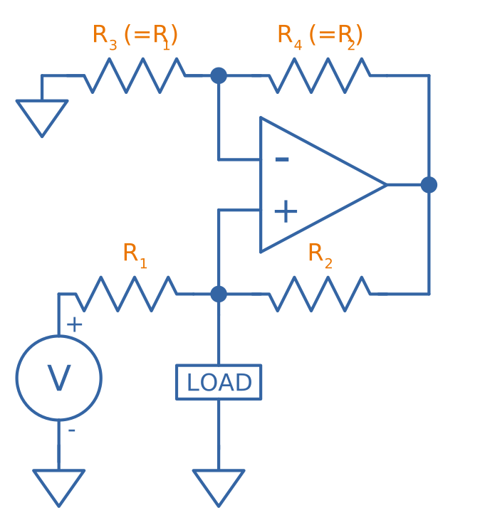
How It Works
First, we’ll annotate the schematic with some labels:
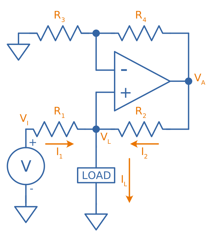
Appling Kirchhoff’s Current Law (KCL) and Ohm’s Law to the circuit, we get:
We also can form a relationship between the voltage at the op-amps non-inverting input and the op-amps output voltage . We can see that it forms a non-inverting amplifier with a gain of :
Now we substitute the expression for directly into the KCL equation and simplify. Notice that in the term the contributions cancel, leaving just , after which we group the terms:
This separates the output current into a driven term and a load-dependent term:
where is the transconductance gain and is the output resistance the circuit presents to the load:
The trick here is to realize we can make the load current independent of the load voltage by driving to infinity (this drives the term ). This requires balancing the bridge so that the denominator goes to zero.
The easy way to do this is to make and , which satisfies automatically:
Setting The Output Current
With the bridge balanced, the load-dependent term drops out and the output current depends only on the input voltage and :
So there are two knobs for setting the current. fixes the transconductance gain (the amps-per-volt), and the input voltage then sets the operating point along that slope. Note that (and its match ) does not appear in this expression — once the bridge is balanced it affects the output compliance and impedance, but not the current.
For example, to source from a input, we need:
and, to keep the bridge balanced, . Keep in mind that the op-amp output must stay within its linear range — if the load voltage climbs high enough to saturate the op-amp, the source can no longer maintain the set current.
The Howland current source is commonly used to build a 4-20mA current-loop transmitter.
Weaknesses
One weaknesses of the basic Howland current source is that it is sensitive to resistor tolerances in the balanced bridge. If the resistors are not well matched, the output current will depend on the load voltage and the output resistance will be finite. This can be mitigated by using precision resistors or trimming the resistors to balance the bridge.1
History
The “Basic Howland Current Pump” was invented by Prof. Bradford Howland in 1962 when working for MIT. It was first published in January 1964 in the “Lightning Empiricist”, Volume 12, Number 1.1 2
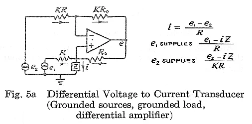
Op-amp Current Sink
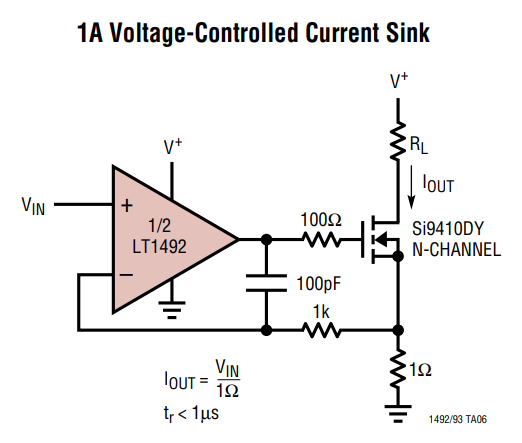
An op-amp, a MOSFET and a sense resistor make a simple and accurate voltage-controlled current sink. Like the Howland source above it converts an input voltage into a proportional output current, but here the load is referenced to the positive supply rail (making it a current sink rather than a ground-referenced source).
The following schematic shows such a device which can control between through the load (shown as ):
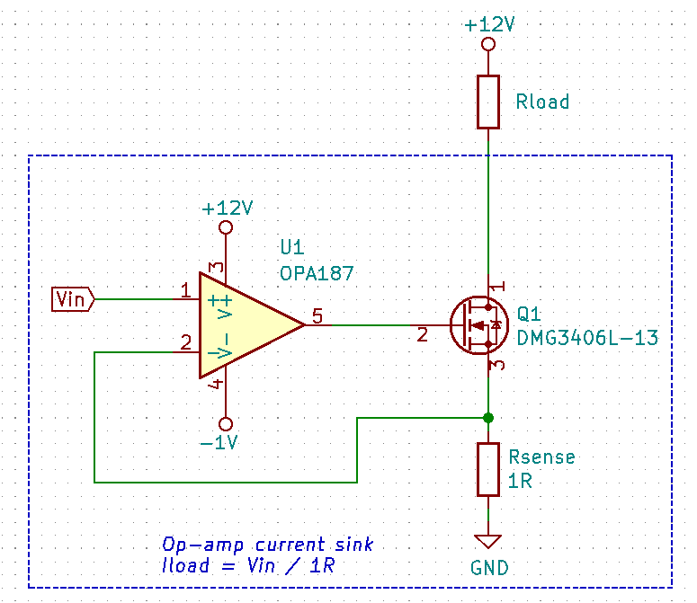
You set the desired load current by providing a voltage to . This voltage typically comes from a resistor divider (fixed current), potentiometer (manually variable current) or DAC (digitally variable current). The load current is given by the simple Ohm’s law equation:
The circuit works like this:
- Desired voltage to set current is provided to which is applied to the positive input of the op-amp, .
- The op-amp will then drive its output high in an attempt to bring its to the same voltage.
- As the op-amp raises the voltage on its output, this is connected to the gate of the MOSFET, which will begin to turn it on.
- As the MOSFET turns on, current begins to flow through the load and sense resistor, .
- The op-amp will keep turning the MOSFET on until the voltage drop across is equal to , meaning is the same as .
- This voltage drop will occur when we have the desired amount of current flowing through it, leading to the equation .
Things to note:
- The op-amp is powered here with a slightly negative voltage rail on its pin. This is so that the op-amp remains operational when you set it at low current levels. At low current levels, the voltages at and are very close to zero. Even rail-to-rail op-amps can have trouble performing well if the negative voltage rail was at .
- The power dissipation through the MOSFET and sense resistor has to be considered. The sense resistor is easy, just make sure it can handle the power given by at the maximum current. The MOSFET power dissipation will depend on the load current and voltage drop across it. The MOSFET is used in its active region --- the region where it is not fully on nor fully off. The MOSFET will drop the remaining voltage from the voltage source provided to the load, once the load voltage drop and sense resistor voltage drop has been subtracted. Use the equation to determine the power dissipation in the MOSFET.
- The gate capacitance of the MOSFET can load the op-amp output to the point that it introduces enough phase lag to cause the circuit to go unstable. See below to recommended compensation circuitry to add to the basic schematic to make the design more stable.
Current Sinking Accuracy
The accuracy of the current sink primarily depends on three aspects:
- The input offset voltage of the op-amp.
- The accuracy of the DAC (or other voltage source) providing the voltage to .
- The tolerance of the current-sense resistor.
MOSFET Gate Capacitance Compensation
The gate capacitance of the MOSFET can load the op-amp output to the point that it introduces enough phase lag to cause the circuit to go unstable. Compensation circuitry can be added as shown in the below circuit to limit the phase lag and prevent the circuit from becoming unstable.
See this Electronics Stack Exchange thread for more information on op-amp stability with capacitive loads.4
Pre-built ICs
XTR111
The XTR111 is a current-loop transmitter by Texas Instruments. It can drive grounded loads. It requires both an external BJT and MOSFET. As of May 2016, this IC was US$1.28 (100).
XTR117
The XTR117 is a current-loop transmitter by Texas Instruments. It cannot drive grounded loads. It only requires an external MOSFET. As of May 2016, this IC was US$1.77 (100).
DigiKey Search
DigiKey stocks a number of pre-built voltage-to-current converter ICs. First, navigate to the following component sub-section on www.digikey.com:
Product Index -> Integrated Circuits (ICs) -> Interface - Sensor and Detector Interfaces.
Then select the filtering options:
- Type: Current Transmitter
- Input Type: Voltage
Footnotes
-
Texas Instruments (2013, Apr). AN-1515 A Comprehensive Study of the Howland Current Pump [application note]. Retrieved 2026-07-14, from https://www.ti.com/lit/an/snoa474a/snoa474a.pdf. ↩ ↩2
-
George A. Philbrick Researches (1964, Jan). The Lightning Empiricist, Volume 12, Number 1 [periodical]. Retrieved 2026-07-14, from http://www.philbrickarchive.org/1964-1_v12_no1_the_lightning_empiricist.htm. ↩ ↩2
-
Linear Technology. LT1492/LT1493: 5MHz, 3V/µs, Low Power Single Supply, Dual and Quad Precision Op Amps [datasheet]. Retrieved 2020-12-25, from https://www.analog.com/media/en/technical-documentation/data-sheets/14923f.pdf. ↩
-
Electronics Stack Exchange (2013, May 16). Stability problem in unity gain opamp [forum post]. Retrieved 2026-06-08, from https://electronics.stackexchange.com/questions/69506/stability-problem-in-unity-gain-opamp. ↩